- 您现在的位置:买卖IC网 > Sheet目录3890 > PIC16C717T-E/SS (Microchip Technology)IC MCU OTP 2KX14 A/D PWM 20SSOP
PIC16C717/770/771
DS41120B-page 108
2002 Microchip Technology Inc.
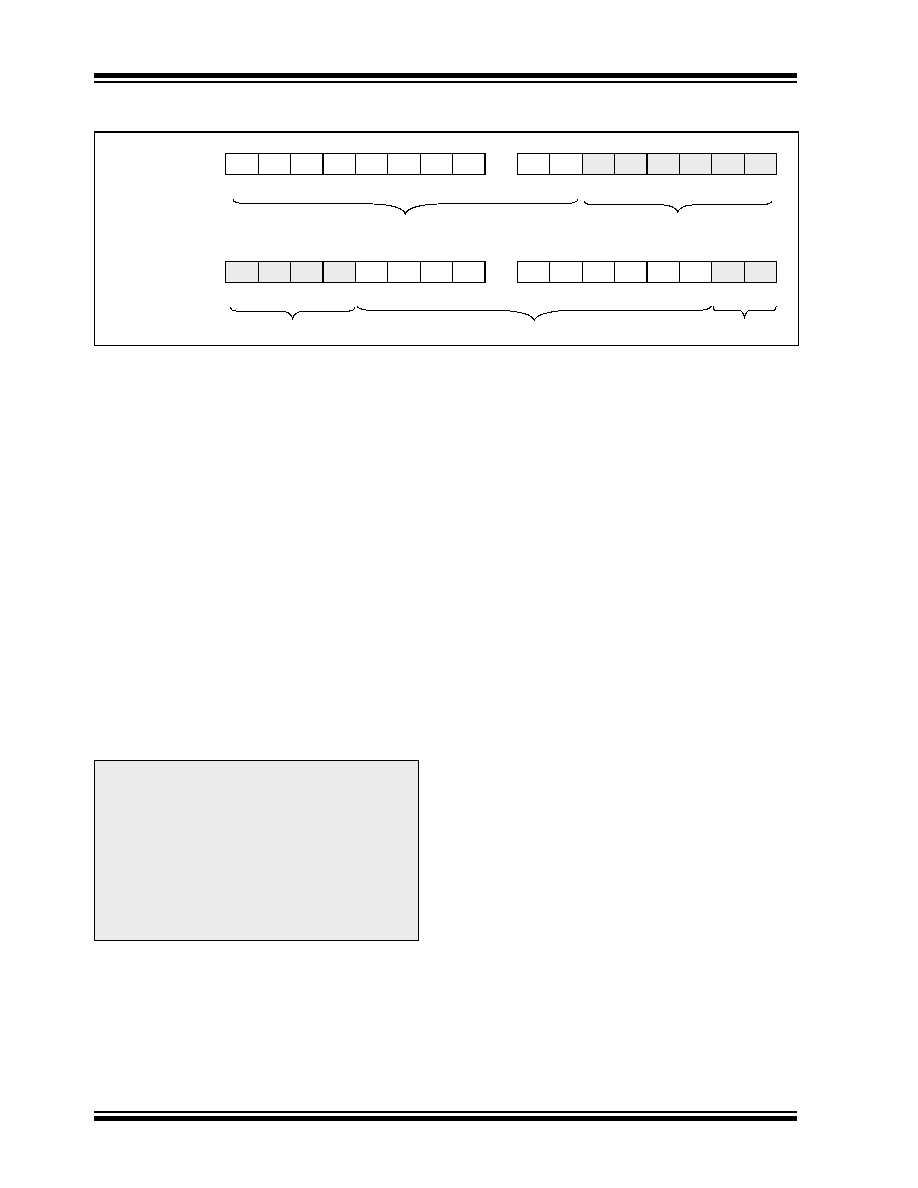
FIGURE 11-2: PIC16C717 10-BIT A/D RESULT FORMAT
After the A/D module has been configured as desired,
the selected channel must be acquired before the con-
version is started. The analog input channels must
have their corresponding TRIS and ANSEL bits
selected as an input. To determine acquisition time, see
Section 11.6. After this acquisition time has elapsed,
the A/D conversion can be started. The following steps
should be followed for doing an A/D conversion:
11.2
Configuring the A/D Module
11.2.1
CONFIGURING ANALOG PORT
PINS
The ANSEL and TRIS registers control the operation
of the A/D port pins. The port pins that are desired as
analog inputs must have their corresponding TRIS bit
set (input). If the TRIS bit is cleared (output), the digital
output level (VOH or VOL) will be converted. The proper
ANSEL bits must be set (analog input) to disable the
digital input buffer.
The A/D operation is independent of the state of the
TRIS bits and the ANSEL bits.
11.2.2
CONFIGURING THE REFERENCE
VOLTAGES
The VCFG bits in the ADCON1 register configure the
A/D module reference inputs. The reference high input
can come from an internal reference (VRH) or (VRL),
an external reference (VREF+), or AVDD. The low refer-
ence input can come from an internal reference (VRL),
an external reference (VREF-), or AVSS. If an external
reference is chosen for the reference high or reference
low inputs, the port pin that multiplexes the incoming
external references is configured as an analog input,
regardless of the values contained in the A/D port con-
figuration bits (PCFG<3:0>).
(ADFM = 0)
MSB
LSB
bit7
10-bit A/D Result
Unused
(ADFM = 1)
MSB
LSB
bit7
Unused
10-bit A/D Result
Unused
Note 1: When reading the PORTA register, all pins
configured as analog input channels will
read as ’0’.
2: When reading the PORTB register, all
pins
configured as
analog
pins
on
PORTB will be read as ’1’.
3: Analog levels on any pin that is defined as
a digital input, including the ANx pins, may
cause the input buffer to consume current
that is out of the devices specification.
发布紧急采购,3分钟左右您将得到回复。
相关PDF资料
PIC16LC770T-E/SO
IC MCU OTP 2KX14 A/D PWM 20SOIC
PIC16C771T/SO
IC MCU OTP 4KX14 A/D PWM 20SOIC
PIC16LC717T-I/SS
IC MCU OTP 2KX14 A/D PWM 20SSOP
PIC16C717T/SS
IC MCU OTP 2KX14 A/D PWM 20SSOP
PIC16LC770T-I/SO
IC MCU OTP 2KX14 A/D PWM 20SOIC
PIC16LC771T-E/SS
IC MCU OTP 4KX14 A/D PWM 20SSOP
PIC16C771T-E/SS
IC MCU OTP 4KX14 A/D PWM 20SSOP
PIC16LC771T-I/SO
IC MCU OTP 4KX14 A/D PWM 20SOIC
相关代理商/技术参数
PIC16C717T-I/SO
功能描述:8位微控制器 -MCU 3.5KB 256 RAM 16 I/O RoHS:否 制造商:Silicon Labs 核心:8051 处理器系列:C8051F39x 数据总线宽度:8 bit 最大时钟频率:50 MHz 程序存储器大小:16 KB 数据 RAM 大小:1 KB 片上 ADC:Yes 工作电源电压:1.8 V to 3.6 V 工作温度范围:- 40 C to + 105 C 封装 / 箱体:QFN-20 安装风格:SMD/SMT
PIC16C717T-I/SS
功能描述:8位微控制器 -MCU 3.5KB 256 RAM 16 I/O RoHS:否 制造商:Silicon Labs 核心:8051 处理器系列:C8051F39x 数据总线宽度:8 bit 最大时钟频率:50 MHz 程序存储器大小:16 KB 数据 RAM 大小:1 KB 片上 ADC:Yes 工作电源电压:1.8 V to 3.6 V 工作温度范围:- 40 C to + 105 C 封装 / 箱体:QFN-20 安装风格:SMD/SMT
PIC16C71T-04/SO
功能描述:8位微控制器 -MCU 1.75KB 36 RAM 13 I/O 4MHz SOIC18 RoHS:否 制造商:Silicon Labs 核心:8051 处理器系列:C8051F39x 数据总线宽度:8 bit 最大时钟频率:50 MHz 程序存储器大小:16 KB 数据 RAM 大小:1 KB 片上 ADC:Yes 工作电源电压:1.8 V to 3.6 V 工作温度范围:- 40 C to + 105 C 封装 / 箱体:QFN-20 安装风格:SMD/SMT
PIC16C71T-04I/SO
功能描述:8位微控制器 -MCU 1.75KB 36 RAM 13 I/O 4MHz Ind Temp SOIC18 RoHS:否 制造商:Silicon Labs 核心:8051 处理器系列:C8051F39x 数据总线宽度:8 bit 最大时钟频率:50 MHz 程序存储器大小:16 KB 数据 RAM 大小:1 KB 片上 ADC:Yes 工作电源电压:1.8 V to 3.6 V 工作温度范围:- 40 C to + 105 C 封装 / 箱体:QFN-20 安装风格:SMD/SMT
PIC16C71T-20/SO
功能描述:8位微控制器 -MCU 1.75KB 36 RAM 13 I/O RoHS:否 制造商:Silicon Labs 核心:8051 处理器系列:C8051F39x 数据总线宽度:8 bit 最大时钟频率:50 MHz 程序存储器大小:16 KB 数据 RAM 大小:1 KB 片上 ADC:Yes 工作电源电压:1.8 V to 3.6 V 工作温度范围:- 40 C to + 105 C 封装 / 箱体:QFN-20 安装风格:SMD/SMT
PIC16C71T-20I/SO
功能描述:8位微控制器 -MCU 1.75KB 36 RAM 13 I/O RoHS:否 制造商:Silicon Labs 核心:8051 处理器系列:C8051F39x 数据总线宽度:8 bit 最大时钟频率:50 MHz 程序存储器大小:16 KB 数据 RAM 大小:1 KB 片上 ADC:Yes 工作电源电压:1.8 V to 3.6 V 工作温度范围:- 40 C to + 105 C 封装 / 箱体:QFN-20 安装风格:SMD/SMT
PIC16C72/JW
功能描述:8位微控制器 -MCU 3.5KB 128 RAM 22 I/O RoHS:否 制造商:Silicon Labs 核心:8051 处理器系列:C8051F39x 数据总线宽度:8 bit 最大时钟频率:50 MHz 程序存储器大小:16 KB 数据 RAM 大小:1 KB 片上 ADC:Yes 工作电源电压:1.8 V to 3.6 V 工作温度范围:- 40 C to + 105 C 封装 / 箱体:QFN-20 安装风格:SMD/SMT
PIC16C72-04/SO
功能描述:8位微控制器 -MCU 3.5KB 128 RAM 22 I/O RoHS:否 制造商:Silicon Labs 核心:8051 处理器系列:C8051F39x 数据总线宽度:8 bit 最大时钟频率:50 MHz 程序存储器大小:16 KB 数据 RAM 大小:1 KB 片上 ADC:Yes 工作电源电压:1.8 V to 3.6 V 工作温度范围:- 40 C to + 105 C 封装 / 箱体:QFN-20 安装风格:SMD/SMT